- Solutions
ENTERPRISE SOLUTIONS
Infuse new product development with real-time intelligenceEnable the continuous optimization of direct materials sourcingOptimize quote responses to increase margins.DIGITAL CUSTOMER ENGAGEMENT
Drive your procurement strategy with predictive commodity forecasts.Gain visibility into design and sourcing activity on a global scale.Reach a worldwide network of electronics industry professionals.SOLUTIONS FOR
Smarter decisions start with a better BOMRethink your approach to strategic sourcingExecute powerful strategies faster than ever - Industries

Compare your last six months of component costs to market and contracted pricing.

- Platform
- Why Supplyframe
- Resources
Modern electronics, from the smartphone in your pocket, to the autonomous features of cutting-edge vehicles, are all made possible by semiconductors that sit at the heart of all modern electronic devices, integrated circuits, and specialized components. With certain chips containing up to billions of semiconductor devices spread across a silicon wafer, one would think that these types of ubiquitous materials should be readily available as a result of their constant demand
What many fail to realize, is that semiconductor manufacturing is costly, complex, and fixed to extended timelines that cannot be easily scaled, or at the very least, not scaled quickly. With shortages in 2021 extending into the second half of the year, join us as we look into the rarely discussed world of semiconductor manufacturing, and the role it plays in navigating present and future shortages.
Semiconductor Shortages: Why We Cannot Simply ‘Make More’
The most recent shortages that began in the fourth quarter of 2020 and extend into 2021 are the result of shifting demand across the automotive and consumer electronics industries, both of whom depend on semiconductors to manufacture their products.
In automotive, this reality comes from a rise in electrification across the vehicle. Not only are electric vehicles on the rise, but technology is prevalent throughout modern automotive designs. From infotainment, to driver-assisted safety features, to power windows and seats, vehicles are closer to computers than they’ve ever been.
This, of course, creates a widespread demand for a variety of different semiconductors. In the face of mounting demand, the simplest solution is to “make more,” but in the case of semiconductors, it’s not that simple.
We recently spoke with Mike Hogan, Senior Vice President and General Manager of the Automotive, Industrial & Multi-market Strategic Business Unit at GlobalFoundries. When asked about issues with capacity and scale, he immediately pointed to the large upfront costs and complexity of scaling something as involved as semiconductor production.
Specifically, the equipment used to build silicon wafers is extremely expensive and built to order. Automotive also presents a unique issue in that additional capacity is required across a wide range of technology nodes. Hogan likens the situation to having a selection of flavors to choose from. “If everyone is buying vanilla, you could simply invest in vanilla.”
The problem arises when you have people buying 30+ flavors and all of them cost 10+ million to increase their capacity by a small margin.
In terms of funding, Mike suggests sharing the upfront costs or changing the pricing on the other side of the equation. Even so, the capacity isn’t going to increase itself. Chip fabs can increase their capacity in bursts, but not every year. Partnerships with customers or governments present a potential avenue to secure additional capacity, but Mike points out that the automotive supply chain hasn’t been tuned to this issue at all in 40+ years of manufacturing, so it’s going to take time and steady demand to balance everything.
In this case, the complexity of the global automotive supply chain provides a wide range of views on how to move forward. From Mike Hogan and GlobalFoundries’ perspective, the automotive industry will move towards a different relationship with their foundry partners, one that is unprecedented for them, but fairly common in electronics.
GlobalFoundries, the only semiconductor manufacturing company with a global manufacturing footprint, is focused on enhancing current nodes at scale, as opposed to chasing 3, 5, or 7 nanometer designs. Ultimately, their goal is creating technology solutions that are more focused on automotive applications as one path forward.
Despite all of this, the fact remains that it can take up to 26 weeks from the start of production, to packaged chips ready for shipment. Furthermore, there are only a finite number of fabrication plants, or fabs, around the world that can produce semiconductors. A deeper dive into how these coveted chips are made offers additional insights into the challenges associated with rising demand and seasons of shortage.
From Silicon to Semiconductor: An Overview of Electronics Component Manufacturing
While most people have heard of semiconductors, very few understand the process of how they are made. As a physical substance that lies somewhere between a conductor and an insulator, semiconductors manage and control the flow of current in electronics. They are often made using raw materials like silicon and germanium, along with other pure elements.
The production involves adding impurities to the base element in a process called “doping,” which adjusts the conductance or inductance of the final outcome based on the type and intensity of added impurities. Computer memory, integrated circuits, diodes, and transistors are all built using semiconductors.
During production, with the exception of Gallium Nitride, all semiconductors are fabricated on single-crystal materials in something similar to the Czochralski method, which was invented in 1915. During this process, molten polycrystalline semiconductor material is combined with a dopant, and then a seed crystal is introduced, which results in the individual atoms arranging themselves to line up with the seed crystal itself.
The crystal is then pulled, polished, and diced into wafers that are polished to the point of being almost completely flat at an atomic level.
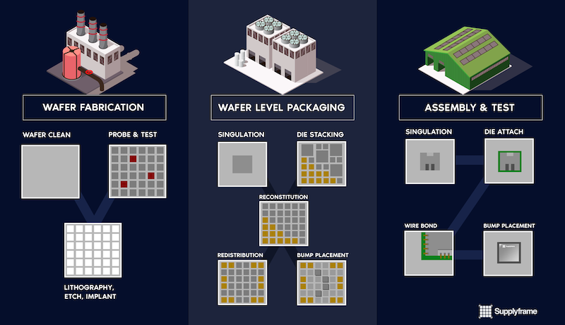
Next is a process known as Photolithography, which uses light to transfer geometric patterns from a photomask to a photosensitive chemical photoresist on the substrate. In practice, this process coats the surface of the wafer with a mask that blocks everything not meant to be exposed to UV light. Once completed, the exposed portion is dissolved, which leaves part of the surface protected and other portions exposed for etching, which traces the shape of wiring and other components.
This entire process establishes a single layer of a circuit, and this description represents a very surface-level description of the process. Depending on the complexity of the manufacturing process, there can be up to 1,400 process steps in the overall manufacturing of the semiconductor wafers alone. Transistors are formed on the lowest layer, but the process is repeated as numerous layers of circuits are formed to create the final product.
Once fabrication is complete, the semiconductors on the silicon wafer must go through assembly, testing, and packaging (ATP) stages of production, which can take an additional six weeks to complete past the 14-20 weeks it takes to manufacture the wafer in the first place.
All of this also occurs within incredibly advanced facilities known as clean rooms, that exist in the central area of a fab. Production usually takes place within hermetically sealed nitrogen environments that utilize automated machinery to transport wafers from one machine to the next.
To maintain these miniature environments that ensure optimal yield in the finished product, fabs require massive amounts of liquid nitrogen as well to maintain the atmosphere within the facility and within specialized sealed boxes known as front opening unified pods, or FOUPs, that are used to transport the wafers.
Charting a Path Forward
Given the complexity of the semiconductor manufacturing process, and the advanced facilities required to manufacture them, it’s easy to see why shortages aren’t as simple as simply scaling capacity. Even so, total global fab capacity will need to increase in the long-term for demand that cannot be met through increased utilization of existing fabs alone.
A combination of record levels of investment into manufacturing and R&D, combined with smarter partnerships and new approaches to procurement will ultimately pave the way forward beyond the present semiconductor shortages.


